4 Layer Pcb Design Rules
You don't have to worry about about track capacitance, emi, decoupling in any other way that you would with 2 layers. For single&double layer pcb, the minimum via diameter is 0.6mm;for multi layer pcb,.
Printed Circuit Board Design Software Free Download
To set up layers in the pcb:

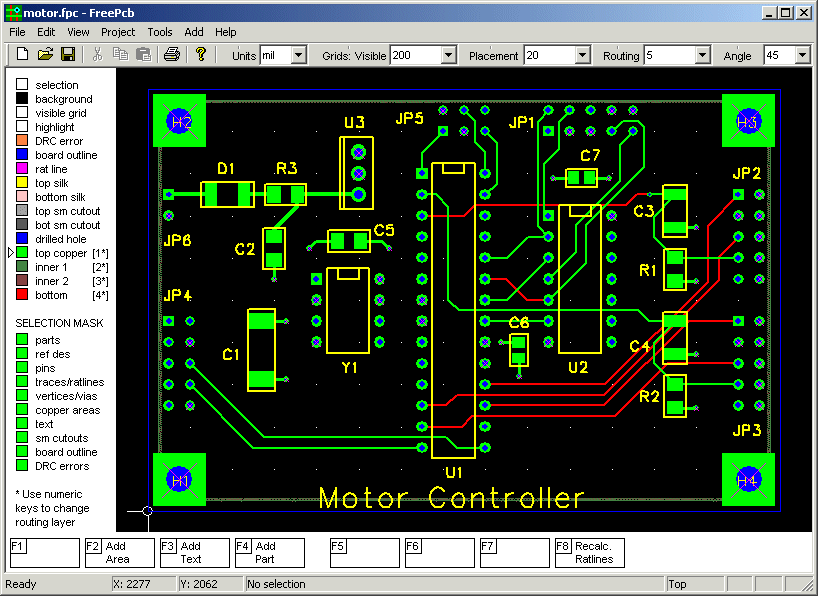
4 layer pcb design rules. Most often, one of these will be a. You can see the top copper layer and the bottom copper layer. The middle layer first uses the command design/layer stack manager to add internal plane1 and internal plane2 with add plane as the most used power layers such as vcc and ground layers such as gnd.
Drc compatible as rule file attached. The top and bottom layers are lay out with signal lines. Select the board setup button.
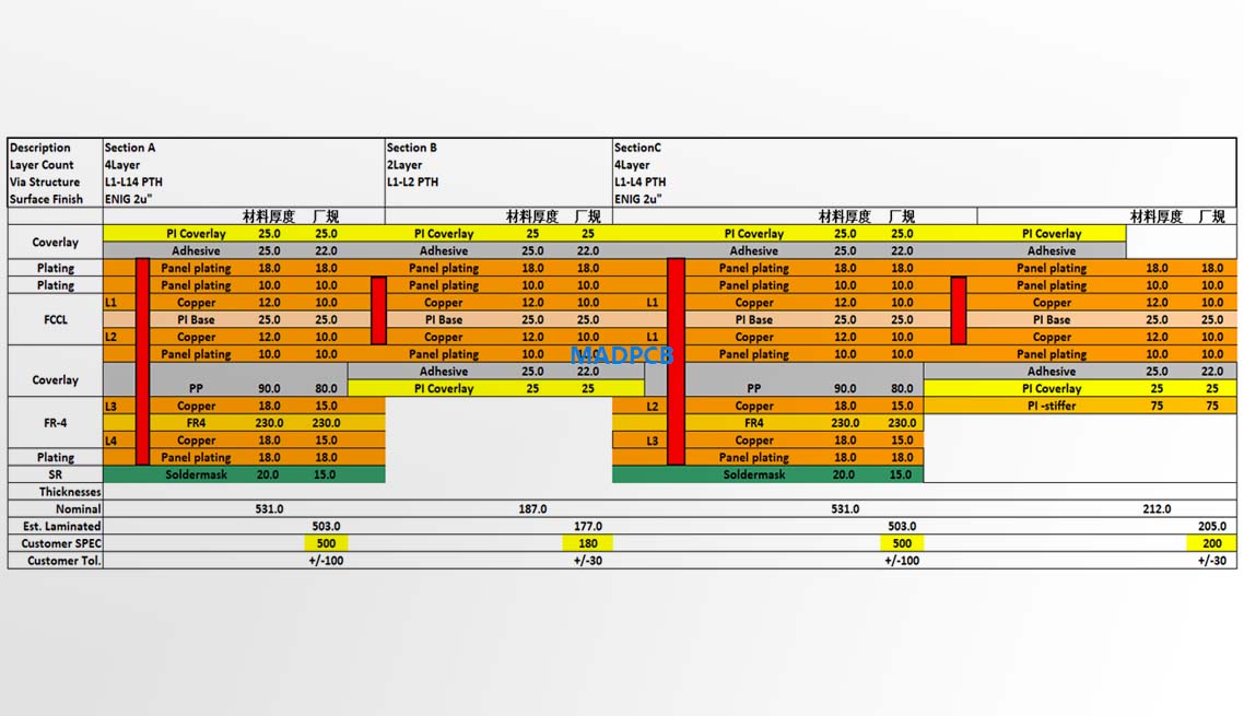
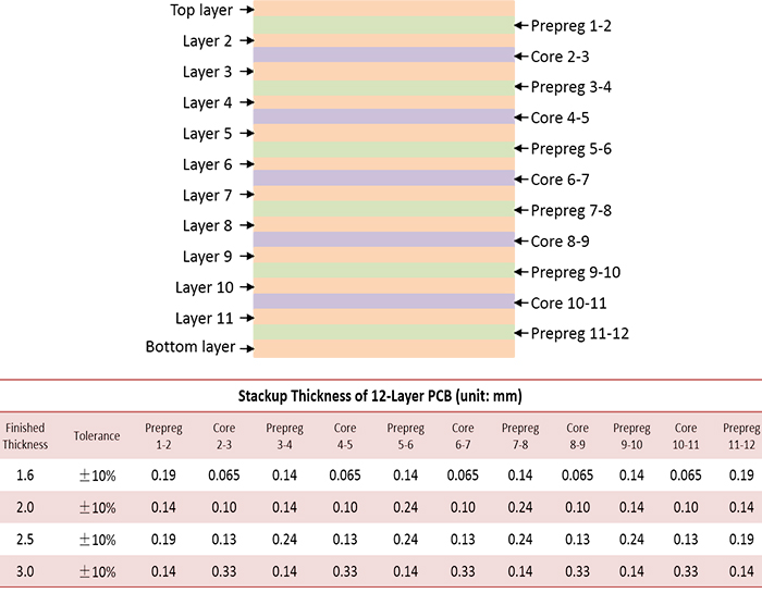
The four layers can be arranged as the top layer being the signal layer; Some guidelines apply specifically to microcontrollers; In this example, as copper thickness is stable, pcb maker will adjust thickness of prepreg and core to meet thickness need.
The holes, hidden holes, and blind holes that link these levels are common. Each zone or board region associates with a specific layer stack. Click board setup at the top.
Take care carefully about that only with high frequencies or projects with specific subtleties. Ideal board stackup from top to bottom is shown in table 1. Altium designer offers advanced pcb layer stack management
Please try to make your pcb width larger than 20mm to reduce manufacturing cost. A pcb layer is made up of signal transmitting levels that are vertical to the board's plane. Lay polysemy lines together as far as possible to increase the grounding area, as neat as possible between the lines.
This means that your board will include blind vias. Resin recession groove is used in board side design instead of. Pcb design must be in the length range (not area) of the dimensions you selected.
For single&double layer pcb, the minimum via hole size is 0.3mm;for multi layer pcb, the minimum via hole size is 0.2mm. However, the guidelines are intended to be general, and apply to virtually a ll modern cmos integrated circuits. The second layer can be the ground layer, the third layer can be set as the power layer, and the last layer can be the signal layer.
One top layer, two inner layers, and one bottom layer. By default, you will have two copper layers. Drills line and long slot cannot be accepted.
As shown in the figure above, a 4 layer stackup includes two internal layers. Type of pcb based on their flexibility sometimes, printed circuit boards are classified based on their flexibility, which defines what applications they can be used for. There're 2 methods to be compatible with the adjustment mentioned above.
Keep out and routing layers finding space for the ground plane and power plane. Although, it is possible to design a 3 layer board with a power plane, practically, a 4 layer pcb, shown in the figure below, is most likely the smallest stackup that will contain a power layer. General layout guidelines for printed circuit boards (pcb), which exist in relatively obscure documents, are summarized.
Generally speaking, 4 layer circuit board includes the top layer, bottom layer, and two middle layers. Professional house painters carefully document the colors and finishes used for. In any case 4 layers offers only advantages.
Protect the board, protect the traces. These four layers are wiring layers to route electrical signals: 4 layers pcb's are almost twice the cost of double layer ones for the same size.
I've known about kicad for years and even tried it once a few years back but it never felt quite "there" yet. Every house has a main electrical service panel or load center that. In layers, you can custom your layer set.
One gerber file, one design.
4 Layer Pcb Design Rules Design Pcbs For Emi Part 2

4Layer RigidFlex PCB with Blind Vias PCB Manufacturer

4 Layer PCB Layout Tutorial,Stackup design,and Cost

Eagle Pcb Software Download

PCBWay Multilayer laminated structure Custom PCB
Simplify your PCB layout When 2 is better than 6 Power

Orcad Pcb Layout How To Set Up A Template Design Dubai

Custom PCB The Ultimate Guide To Getting The Best

Standard 4 and 6Layer PCB Stackups BitWeenie BitWeenie

PCB Design Rules Check Fails fab fritzing forum
4 Layer Pcb Design Rules Design Pcbs For Emi Part 2
BGA Design in 4 layer PCB Circuit Routing and Pin

4 Layer Pcb Design Rules PCB Designs
4 Layer Pcb Design Rules PCB Designs

Pcb Layout 4 Layer PCB Circuits

4 Layer Pcb Layout Guide PCB Board

4 Layer Pcb Design Rules Design Pcbs For Emi Part 2
4 Layer Pcb Layout PCB Designs

DesignLeitlinien Eurocircuits
